
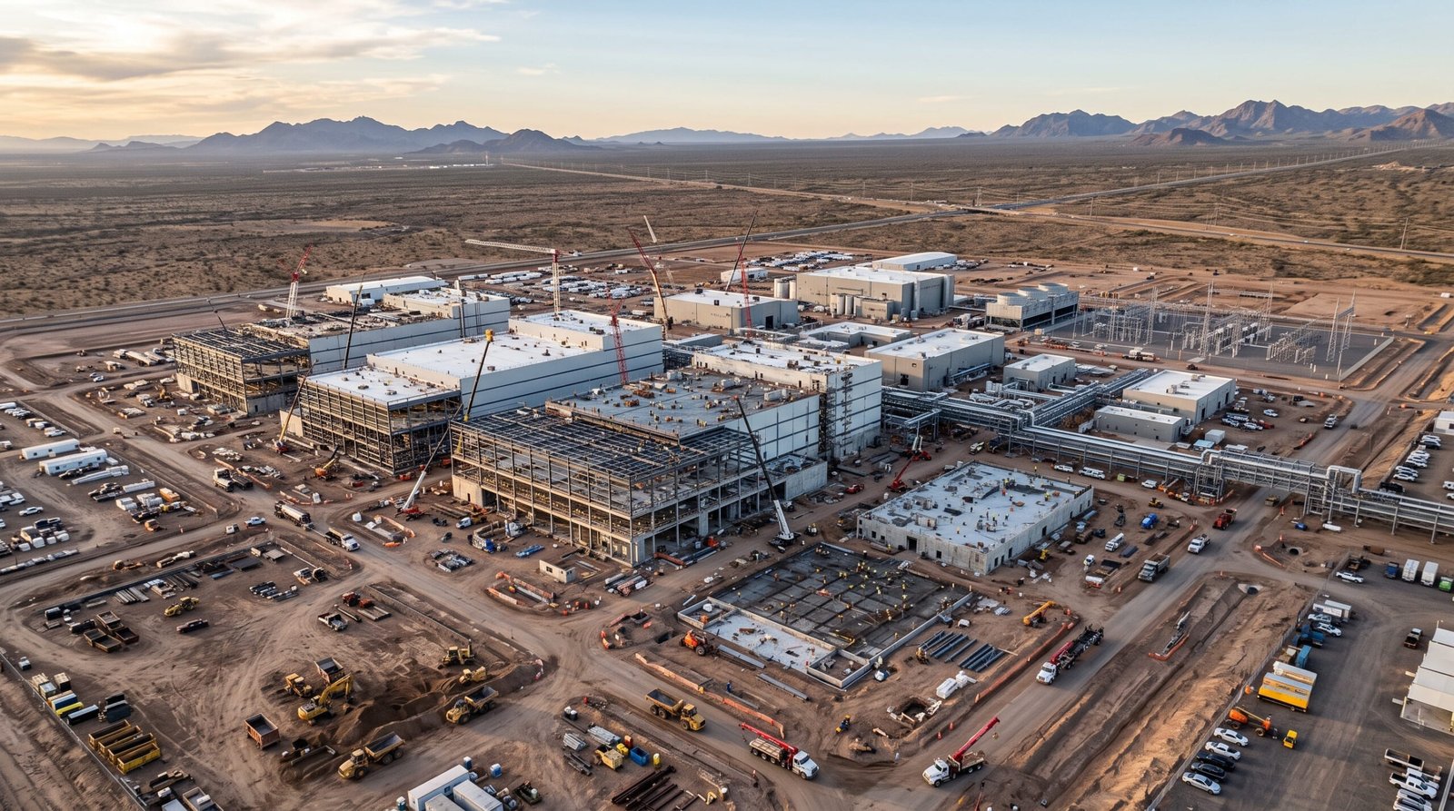
Semiconductor fab relocation is happening at a scale and speed that has no historical precedent. In January 2026, the US and Taiwan signed a trade and investment agreement under which Taiwanese semiconductor and technology enterprises committed at least $250 billion in new direct investment in the United States. TSMC alone has now committed $265 billion for its Arizona campus, targeting six wafer fabs, two advanced packaging facilities, and an R&D centre. Amkor Technology broke ground on a $7 billion advanced packaging campus in Peoria, Arizona in October 2025. GlobalFoundries is executing a $16 billion reshoring programme across its US facilities. The IndustrialSage US Manufacturing Investment Tracker, as of July 20, 2026, is tracking $1.917 trillion in announced private-sector US manufacturing and industrial investment commitments across 164 companies.
Simultaneously, Asia is not standing still. In India, 13 semiconductor projects are approved or operational under the India Semiconductor Mission. Tata Electronics is targeting first silicon at its Dholera, Gujarat fab by late 2026, partnering with PSMC of Taiwan, supported by ASML on lithography equipment. Micron’s $2.75 billion OSAT facility in Sanand, Gujarat is packaging and testing DRAM and NAND chips at volume. Japan’s Rapidus is building a 2nm fab in Hokkaido. Singapore, South Korea, and Germany are all adding capacity simultaneously.
What none of these announcements describe in detail is the physical reality that sits behind every single one: moving a semiconductor fabrication facility, or even moving equipment into one, is the most technically demanding, highest-precision, highest-consequence physical relocation task in modern manufacturing. This guide covers what is actually shifting, what it costs, and what the equipment relocation layer inside this global story demands.
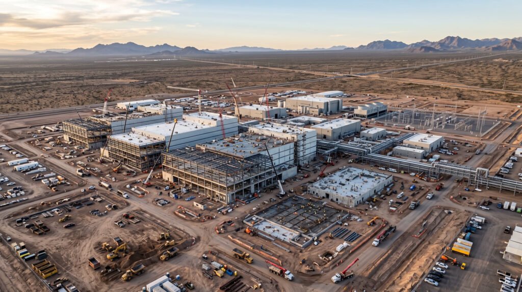
Table of Contents
- Semiconductor Fab Relocation: The Global Map in 2026
- TSMC Arizona: The Centrepiece of the US Reshoring Story
- Amkor, GlobalFoundries, and the Advanced Packaging Shift
- India’s Semiconductor Fab Moment: Dholera, Sanand, and the ISM Pipeline
- What Semiconductor Fab Equipment Relocation Actually Involves
- Why Fab Equipment Moving Is the Highest-Precision Relocation Task in Manufacturing
- What Enterprises and Supply Chain Partners Must Do Right Now
- How One World Logix Supports Semiconductor Fab Relocation Projects
1. Semiconductor Fab Relocation: The Global Map in 2026
The global semiconductor industry is executing the most expensive supply chain diversification in history, driven by three converging forces: US-China geopolitical decoupling, the Taiwan Strait concentration risk that became undeniable after 2022, and the CHIPS Act’s $52.7 billion in domestic manufacturing subsidies which activated billions in private investment alongside it.
As of April 2026, 65 semiconductor fabrication facilities are tracked across 10 countries, operated by 16 companies including TSMC, Samsung, Intel, SMIC, Rapidus, GlobalFoundries, UMC, Tower, and others, with 42 operational fabs, 13 under construction, and 2 announced. The concentration risk that made this shift inevitable is visible in the same data: leading-edge fabs remain heavily concentrated in Taiwan, South Korea, and now, increasingly, Arizona.
As of July 20, 2026, the IndustrialSage tracker covers $1.917 trillion in announced private-sector US manufacturing and industrial investment commitments across 164 companies and 37 states. The largest semiconductor investors include TSMC at $265 billion, Micron at $250 billion, and Texas Instruments at $60 billion. This is not a policy document. It is capital already in motion, across construction sites, equipment orders, and facility conversions.
2. TSMC Arizona: The Centrepiece of the US Reshoring Story
No single semiconductor fab relocation story defines 2026 more clearly than TSMC’s Arizona expansion.
TSMC’s first Arizona fab, Fab 21 Phase 1, is now operational and producing advanced chips for Apple and NVIDIA, including chips for NVIDIA’s Blackwell AI processors, marking the first time TSMC has produced cutting-edge AI silicon outside of Taiwan. The second fab, Fab 21 Phase 2, has completed construction ahead of schedule. TSMC plans to begin moving chipmaking equipment into the facility in Q3 2026, with high-volume 3nm production targeted for 2027. This timeline was accelerated by a full year from the original 2028 target, due to surging demand from AI chip customers.
TSMC will spend an additional $100 billion building fabs in Arizona, which takes the company’s total US investment to $265 billion. The expansion covers several semiconductor logic wafer fabs for 2-nanometer and below technologies, as well as advanced packaging fabs. TSMC’s plans in Arizona now include six wafer fabs, two advanced packaging facilities, and an R&D centre.
Under the US-Taiwan deal, Taiwanese semiconductor and technology enterprises committed at least $250 billion in new direct investment in the United States, while Taiwan also pledged at least $250 billion in credit guarantees to support further expansion. The Arizona gigafab cluster is not just a semiconductor facility. It is the physical expression of a geopolitical strategy.
3. Amkor, GlobalFoundries, and the Advanced Packaging Shift
TSMC is the headline, but the semiconductor fab relocation story extends well beyond wafer fabrication into the advanced packaging layer that completes the chip production process.
Amkor Technology officially broke ground on its expanded advanced packaging and test campus in Peoria, Arizona in October 2025. The $7 billion investment establishes the nation’s first high-volume advanced packaging facility, cementing America’s position in the final and increasingly critical stages of chip production. Amkor is projecting 2026 capital expenditure between $2.5 billion and $3 billion, with the Arizona campus as the centrepiece of its expansion.
GlobalFoundries is executing a $16 billion US reshoring programme across its New York and Vermont facilities, targeting mature-node and specialty chip production that AI accelerators and automotive chips both depend on. Intel received $8.5 billion in CHIPS Act subsidies for its Arizona and Ohio fabs and remains a critical domestic partner in the reshoring ecosystem.
The advanced packaging layer is where the physical relocation challenge is most immediate. TSMC’s plans to begin moving chipmaking equipment into Fab 21 Phase 2 in Q3 2026 means that semiconductor fab equipment relocation is happening on construction sites in Arizona right now, this quarter, at the precise moment this blog is published.
4. India’s Semiconductor Fab Moment: Dholera, Sanand, and the ISM Pipeline
While Arizona dominates the reshoring narrative, India’s own semiconductor fab construction is reaching its most consequential phase simultaneously.
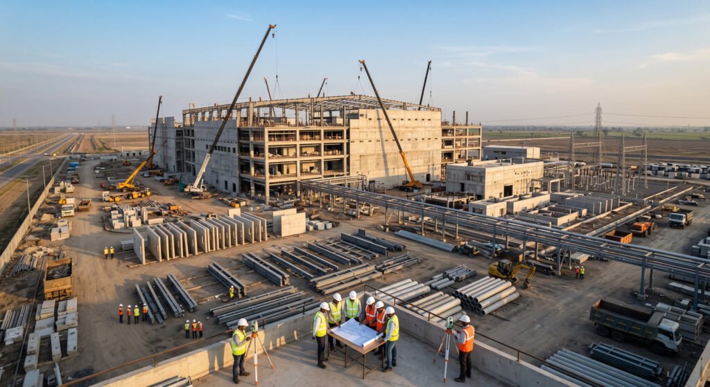
Tata Electronics’ Dholera fab carries a total investment of Rs 91,000 crore, with the central government contributing 50 percent of capex. First silicon is targeted for December 2026, per Union Minister Ashwini Vaishnaw’s confirmed timeline. Tata Electronics and ASML signed a strategic agreement on May 16, 2026, to support the development of India’s first front-end semiconductor fabrication facility in Gujarat, covering lithography equipment supply, talent development, and supply chain collaboration.
Micron’s $2.75 billion OSAT facility in Sanand, Gujarat began volume production in late 2025, packaging and testing DRAM and NAND flash memory chips for global markets. Tata Electronics’ semiconductor assembly and test facility in Jagiroad, Assam is operational. CG Power’s OSAT facility in Sanand, developed with Renesas of Japan and Stars Microelectronics of Thailand, is coming online targeting automotive-grade chip production.
As of July 2026, 3 of 12 approved commercial facilities are now operational. Total approved investment across all India Semiconductor Mission projects stands at Rs 1,65,573 crore across 6 states. A Tower Semiconductor and Adani Group joint venture is planned for Taloja in Panvel, Mumbai. India Chip, an HCL-Foxconn Group joint venture, has broken ground at YEIDA, Jewar, Uttar Pradesh. India’s Budget 2026 allocated Rs 8,000 crore to the semiconductor mission, its largest single-year allocation.
5. What Semiconductor Fab Equipment Relocation Actually Involves
Every fab expansion, every equipment move-in, and every cross-border relocation of semiconductor production machinery sits behind a physical logistics challenge that most supply chain analyses skip entirely.
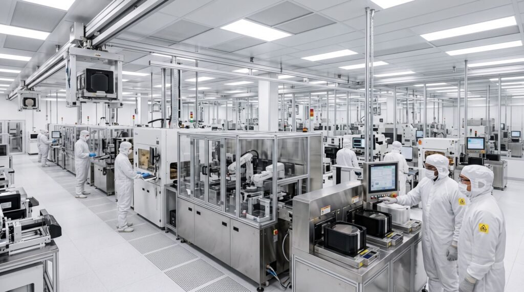
A semiconductor fabrication facility contains equipment categories that exist nowhere else in manufacturing. Photolithography scanners, chemical vapour deposition chambers, ion implanters, etching systems, chemical mechanical planarisation tools, and metrology equipment are all precision instruments where tolerances are measured in nanometres. A vibration event during transport that would be imperceptible to the human body can permanently misalign an optical component inside a lithography tool that costs $50 million to $400 million to replace.
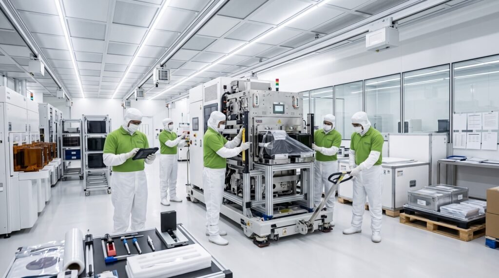
These machines cannot simply be loaded onto a flatbed and driven to a new site. Each tool requires a defined move procedure, including vibration monitoring throughout transport, temperature and humidity-controlled containers, anti-static packaging for electronic assemblies, and clean-environment reinstallation at the destination. The move procedure for a single advanced lithography tool can run to hundreds of pages of documented protocol.
At destination, every tool goes through an installation qualification, operational qualification, and performance qualification sequence, referred to as IQ/OQ/PQ, before it can be used in production. This validation process for a single complex tool can take 4 to 12 weeks. Multiply that across the 500 to 1,000 tools a modern leading-edge fab contains, and the logistical and timeline complexity becomes apparent.
6. Why Fab Equipment Moving Is the Highest-Precision Relocation Task in Manufacturing
The gap between a standard industrial machine shift and a semiconductor fab equipment relocation is not a matter of degree. It is a completely different discipline.
A standard CNC machining centre relocation requires vibration-dampened transport and careful levelling at the new site. A semiconductor lithography scanner requires a move procedure that includes real-time vibration monitoring during every phase of transport, clean room-compatible packaging and handling at both ends, an installation sequence that must follow the equipment manufacturer’s exact protocol, and a full performance qualification before the first wafer runs.
Crane handling for fab equipment also operates at a different precision level. Overhead bridge cranes inside a cleanroom environment must meet ISO 14644 cleanliness standards. Any particulate contamination introduced during equipment movement can affect yield across an entire production lot.
For equipment being relocated internationally, from Taiwan to Arizona, from India to the United States, or between Asia-Pacific facilities, the logistics layer adds customs documentation aligned with dual-use export control regulations, ECCN classification for controlled semiconductor equipment, and import compliance at the destination port. A misstep in export documentation for controlled semiconductor equipment can halt an international equipment move for months.
7. What Enterprises and Supply Chain Partners Must Do Right Now
The semiconductor fab relocation wave creates cascading opportunity and risk for the entire supply chain ecosystem around these facilities.
For equipment vendors, chemical suppliers, and logistics partners servicing fabs in Arizona, Gujarat, Hokkaido, or Singapore, the construction timelines are live right now. TSMC’s Fab 21 Phase 2 equipment move-in begins Q3 2026. Tata’s Dholera fab targets first silicon by late 2026. These are not future deadlines. They are active windows.
Companies that want to be positioned as approved vendors or logistics partners for these campuses need to begin qualification conversations now, not after the first tool move-in has already happened. Fab operators run approved vendor lists for logistics and equipment handling that take months to qualify onto.
For enterprises running their own semiconductor supply chain operations and evaluating whether to relocate production capacity closer to a new regional fab cluster, whether in Gujarat, Arizona, or Southeast Asia, a physical site assessment of current equipment and a realistic cost and timeline model for the move is the essential first step before any commercial decision.
8. How One World Logix Supports Semiconductor Fab Relocation Projects
One World Logix (OWL), headquartered in CBD Belapur, Navi Mumbai, brings 14 years of precision machine shifting, cross-border freight, and factory relocation experience to the semiconductor fab relocation projects that are now underway across India and globally. As India’s Zero-Downtime Migration Specialists, OWL operates across 30 countries with the international freight, customs clearance, and precision equipment handling capability that semiconductor fab equipment moves demand.
OWL’s semiconductor and high-precision equipment relocation capability covers pre-move site survey and equipment documentation, vibration-monitored transport with real-time logging, clean-environment handling and packing protocols, international ocean and air freight with dual-use export documentation, and reinstallation support at the destination facility. OWL holds ISO 9001:2015 certification and is a member of IAM and GEM, the international standards bodies for migration.
With India’s Dholera fab targeting first silicon in late 2026, the Tower-Adani fab planned for Taloja in Mumbai’s backyard, and Micron’s Sanand facility already operational, the semiconductor fab relocation opportunity in India is no longer theoretical. It is operational, active, and within OWL’s geographic core.
If your organisation is planning equipment moves related to a semiconductor fab setup, expansion, or cross-border relocation, start with a free on-site assessment. No commitment, no cost.
Contact One World Logix today:
Phone: +91-88288 20887
Email: info@oneworldlogix.com
Website: oneworldlogix.com/owl/
Book your free semiconductor equipment relocation assessment. The global chip map is being redrawn. Make sure your equipment move is executed with the precision this industry demands.